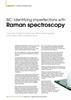
반도체
현대 전자 산업에서는 광범위한 반도체 물질을 사용합니다. 트랜지스터, 태양 전지, 발광 다이오드 등의 첨단 기기는 재료 특성의 한계를 뛰어 넘게 하며, 극도로 균질한 원자재를 필요로 합니다. 라만 분광기는 반도체 연구에 적합한 도구입니다.
반도체 특성 규명
라만을 사용하면 모든 반도체(예: Si, 탄소계, III-V 및 폴리머) 및 초전도체의 특성을 규명하고 이미지를 생성할 수 있습니다. 다음을 포함하여 다양한 정보를 확인할 수 있습니다.
- 화학적 조성(예: 화합물 반도체 중 합금 성분)
- 다형체 결정(예: 4H-SiC, 6H-SicC)
- 압력/응력
- 도펀트 농도
- 박막 두께
- 결정 구조 유형 및 방향
- 결정성
- 균일성 및 순도
- 장치 온도

간편한 분석
샘플 준비 작업이 불필요하기 때문에 라만 분석은 간단합니다. 진공 기술도 필요하지 않고, 전자 현미경에서 충전 효과로 인한 문제도 발생하지 않습니다.
Renishaw는 연구 과학자부터 기술자에 이르기까지 모든 사용자에게 적합하도록 라만 시스템을 구성할 수 있습니다.
넓은 영역 분석
Renishaw 라만 시스템은 매우 큰 샘플을 분석할 수 있습니다. 예를 들어, 전체 웨이퍼 이미지를 생성하여 오염물이나 잔류 응력을 알아낼 수 있습니다.
PL 특성 규명
Renishaw 라만 시스템을 사용하여 광발광(PL) 스펙트럼을 수집하고 분석할 수도 있습니다. 하나의 계기로 진동 정보와 전자 정보를 모두 수집할 수 있습니다.
온라인 시스템
품질 관리 목적으로 온라인 분석을 수행하려면 생산 라인에 Renishaw 라만 시스템을 추가하십시오. 조기에 문제를 진단하여 폐기물을 줄이고 수율을 향상시킬 수 있습니다.
신뢰할 수 있는 결과
Renishaw 라만 시스템은 반복정도가 뛰어나서 샘플을 정확히 대표하는 데이터를 생성합니다. 내장된 자동 캘리브레이션 및 상태 점검 기능을 통해 데이터의 수집 시기에 관계없이 데이터를 정확히 비교할 수 있습니다.
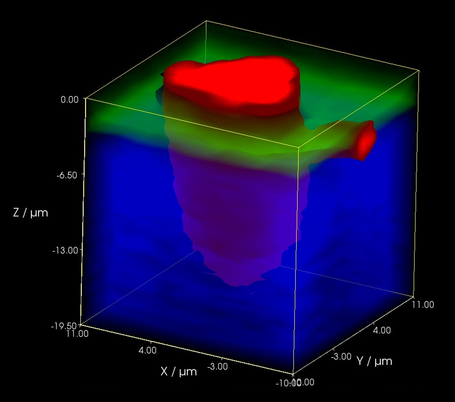
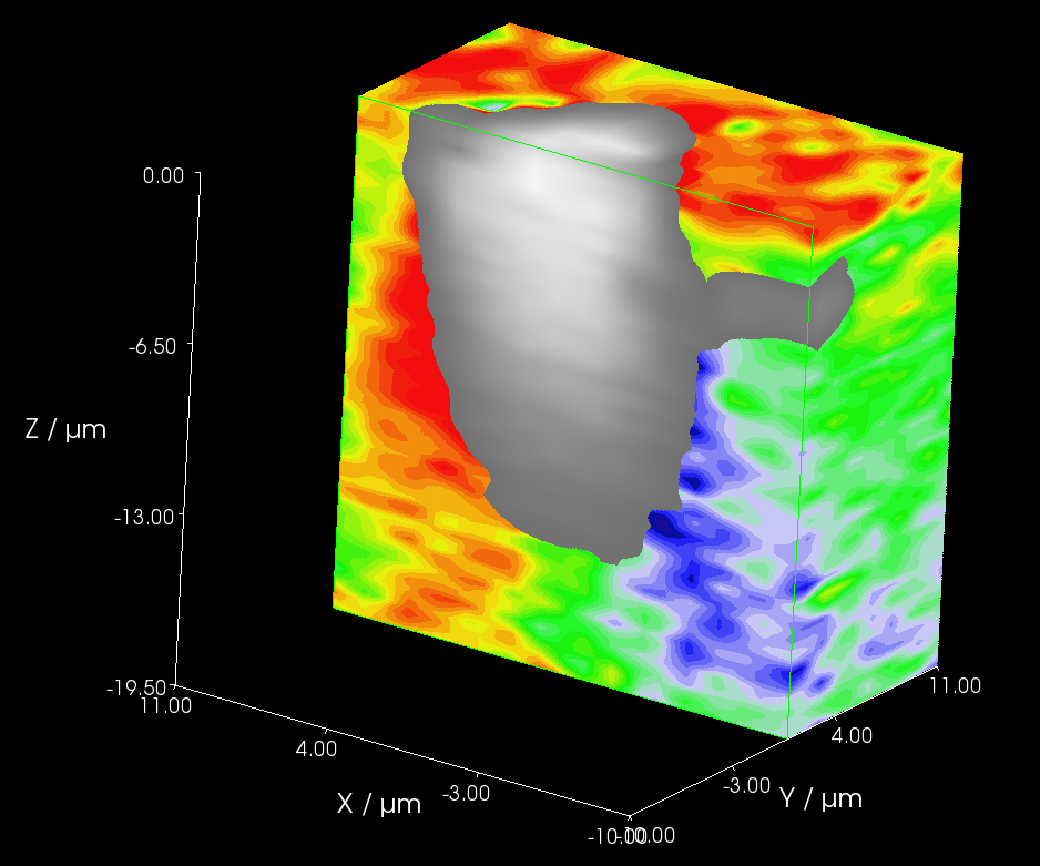
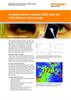
실리콘 카바이드 웨이퍼에 대한 3D 라만 지도
다운로드: 재료 과학(반도체)
-
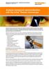
 Application note: Photocurrent measurements on the inVia™ confocal Raman microscope [en]
When light interacts with semiconducting materials it can induce electrical currents (‘photocurrents’). These currents carry information about the electronic, optical, and charge transport properties of the material. This information is complementary to that obtainable from Raman scattering, which can identify physical changes in the material properties. This application note demonstrates the capability to simultaneously collect Raman and photocurrent data using the photocurrent mapping module concurrently with an inVia Raman microscope.
-
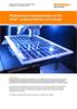
 Application note: Analyse compound semiconductors with the inVia™ Raman microscope [en]
Over the last decade compound semiconductors have attracted a great deal of attention because they offer properties suitable for next generation devices in a wide range of application areas. Historically, the fabrication of these devices has been hindered by material challenges. While these have mainly been conquered at the research level, problems still persist when scaling up to industrial production. Renishaw’s inVia Raman microscope is a non-invasive, non-destructive characterisation tool which provides sub-micrometre information on the vibrational, crystal and electronic structure of materials.
-
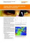 Application note: Analyse silicon carbide (SiC) with the inVia Raman microscope [en]
The properties of silicon carbide are highly dependent on its crystal structure (it can exist in many polytypes), on the quality of the crystal, and on the number and types of defects present. Manufacturers of silicon carbide raw material and devices need to monitor and control these attributes to enhance yield. The first step in controlling these parameters is to measure them repeatably and quantifiably. Renishaw’s Raman systems are ideal for this.
-
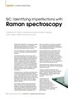 News release: Identifying imperfections with Raman spectroscopy [en]
An article in Compound Semiconductor magazine, October 2015, describes how Raman spectroscopy allows routine mapping of SiC wafers in little more than an hour.
관련 스토리
inVia을 활용하여 세계 에너지 문제를 해결하기 위해 작업 중인 Caltech
캘리포니아공과대학(Caltech)에서 햇빛과 물, 이산화탄소만으로 태양 연료를 생산하는 새롭고 효과적인 방법을 찾고 있습니다. 이 연구에서는 광 촉매 반응과 광 포획 조사에 초점을 맞춥니다.
Renishaw의 inVia, CS Industry Award 2016 수상 제품으로 선정
글로벌 엔지니어링 기술 기업인 Renishaw에서 CS Industry Award 2016의 계측 부문 수상 제품으로 inVia 라만 현미경이 선정되었음을 발표했습니다. Compound Semiconductor 매거진이 주관하는 CS Industry Awards는 웹사이트(www.compoundsemiconductor.net)에서 투표를 통해 수상 제품을 선정하며 폭넓은 화합물 반도체 산업 제품을 대상으로 수상 제품을 가립니다.